The 19th AMB will be held in Shenzhen from October 28th to 30th. In the International Pavilion of Hall 6, we will see a lot of upstream suppliers in the supply chain, many of which are lens and sensor manufacturers.
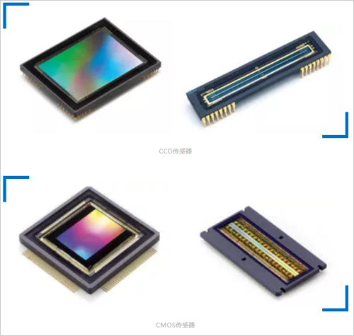
The core technical components of the video surveillance system are optical imaging devices, while the optical imaging devices mainly include lenses and photosensitive devices. Currently, the photosensitive devices are mainly CCD and CMOS.

CCD (Charge Coupled Device) and CMOS (Complementary Metal Oxide Semiconductor) image sensors are two different devices for acquiring digital images. Both have advantages and disadvantages and have their own advantages in different applications.
There have been many discussions about the relative advantages of CMOS over CCD. The debate has been going on for a long time, but there is no clear conclusion. This is not surprising, because the problem is not static.
Technology and market development are not only affecting what is technically feasible, but also affecting what is commercially viable. The application of imaging devices is varied and the needs are constantly changing.
First, both CCD and CMOS imaging rely on the photoelectric effect to generate an electrical signal from light. Both types of imaging element principles convert light into electrical charge and process it into an electrical signal.
In a CCD sensor, the charge of each pixel is transmitted through a very limited number of output nodes (usually only one), then converted to voltage, buffered and sent out of the chip as an analog signal. All pixels can be used for light capture, and the uniformity of the output (a key factor in image quality) is high.
In CMOS sensors, each pixel has its own charge-to-voltage conversion, and the sensor typically also includes an amplifier, noise correction, and digitization circuitry for the chip to output a digital signal. These other features (compared to CCD) increase design complexity and reduce the area available for capturing light. When each pixel is converted, the uniformity is reduced.
Both CCD and CMOS imagers were invented in the late 1960s and 1970s. CCDs dominated at the beginning, mainly because they can provide outstanding images using existing manufacturing techniques. CMOS image sensors require higher consistency and smaller manufacturing processes that were not available at the foundry of the time.
Until the 1990s, lithography was developed to allow designers to consider the CMOS. A renewed focus on CMOS is based on considerations such as reducing power consumption, increasing integration, and reducing manufacturing costs by multiplexing mainstream logic and memory devices. After investing a lot of time, money and process improvements, CMOS has met these expectations in actual production, and has become a mature mainstream technology.
In the case of coexistence of the two, some applications can achieve better results using CMOS, and in some cases CCD. By comparing different situations, we can understand the technical tradeoffs and some cost considerations.
Imaging of video equipment
With lower power consumption and higher integration, smaller components, CMOS has succeeded in imaging mobile phones. In order to develop and fine-tune CMOS imagers and their manufacturing processes, upstream companies in the semiconductor industry have invested heavily, and as pixel size has shrunk, image quality has improved significantly.
Therefore, in the field of consumer electronics and video surveillance, CMOS imaging performance is superior to CCD based on almost all performance parameters.
Machine vision imaging
In machine vision, thanks to the huge investment in mobile phone imaging, the development of CCD is also a technology in the field of surface scanning and line scanning devices in most machine vision fields.
For machine vision, the key parameters are speed and noise. The difference between CMOS and CCD imaging is that the signal is converted from a charge to an analog signal, and the way it is converted to a digital signal is different.
In CMOS, the front end of the data path is highly parallel. This allows each amplifier to have a low bandwidth. In contrast, high-speed CCDs have a certain amount of parallel output channels, but they do not have as many parallel analog front ends as high-speed CMOS, allowing for massively parallel processing.
However, there are exceptions. Under what circumstances is CCD better than CMOS?
Near infrared imaging
To image in near-infrared light (wavelengths of 700 to 1000 nm), the imager needs to have a thicker photon absorption region. This is because the infrared photons are deeper than the absorption regions of the visible light in the silicon.
Most CMOS imager manufacturing processes are adjusted for imaging only in visible light. So these imagers are less sensitive to near infrared (NIR). To increase the substrate thickness and change the doping level, it will affect the operation of CMOS analog and digital circuits.
CCD manufacturing ensures a thicker substrate thickness while retaining its normal working ability. Therefore, CCDs specifically designed to image in near-infrared light are much more sensitive than CMOS.
Time delay and integral imaging
Time delay and integral (TDI) imaging. Commonly used in machine vision and remote sensing, its operation is very similar to line scan imagers. When the image of the subject is scanned progressively, each line captures a snapshot of the object. TDI is useful when the signal is very weak, because multiple snapshots of the subject are added together to create a stronger signal.
Currently, CCD and CMOS TDI have different ways of superimposing multiple snapshots. The CCD combines the signal charge while the CMOS TDI incorporates the voltage signal. The summation operation is noise-free in the CCD, but not in CMOS. When the number of rows of CMOS TDI exceeds a certain number, the noise from the summing operation is superimposed, so that the advanced CMOS TDI cannot obtain less noise than the ordinary CCD TDI.
Electron multiplying imaging
The Electron Multiplying CCD (EMCCD) is a CCD device whose structure limits the noise added by the signal during the multiplication process. This will result in a net signal-to-noise ratio (SNR) gain, so in applications where the signal is weak, EMCCD can detect several scientific imaging. EMCCD can therefore be used for ultra-low signal applications, typically for scientific imaging.
Cost consideration
In reality, for many business decisions, the technical and performance-based trade-offs that are specific to the situation are more about the performance of the price paid.
First, develop and customize costs. The development of CMOS imagers is often more expensive because CMOS uses more expensive deep sub-micron masks. More circuits need to be designed in CMOS devices, so the development cost of CMOS devices is higher.
Second, the quantity determines the cost of production. Although the cost of developing a new CMOS imager is higher, it is possible to take advantage of the increase in scale to reduce the CMOS unit production cost. In high-volume production applications, lower unit production costs are more important in terms of financially lower overall development costs.
Third, supply stability is important. It is terrible and expensive to design peripheral circuits around imaging devices that may be discontinued. Therefore, it is necessary to choose a company that has the ability to produce imaging devices for a long time, and currently CCD has gradually withdrawn from the market, CMOS. At present, CCD is gradually being withdrawn from the market, and CMOS solutions are being adopted more and more, and stable supply has helped it become a mainstream imaging device.
Summary: CMOS has become mainstream
A variety of applications have different requirements. These requirements impose constraints that affect performance and price. The trade-off between price and performance, as well as the number of applications and supply stability, will affect the choice of CMOS and CCD. Due to these complexities, it is not possible to make a general statement of CMOS and CCD imaging for all applications.
However, in most visible light imaging applications, CMOS imaging outperforms CCDs, which is why CMOS has gradually replaced CCDs in most applications. But for some special cases, such as time delay and integral imaging when the signal is weak, near-infrared NIR imaging, scientific imaging, CCD is still a better choice.
Vertical Pop Up A- Frame Banner
Description
:
Vertical pop up a –frame banner includes 2
panels and 3 panels tower pop up a frame banners. The 3 Panel Tower Pop Up banner is easy to use
and offers a large branding area times 3! Its easy to use technology makes it a
'must' addition to your range of events and branding signage.

Specification :
Application :Two panels
vertical pop up a frame banners :
Size list
:
Small
:60*90 cm ; Medium :100*170 cm ; Large :125*200 cm
Material : 280 g soft elastic tension fabric with dye sublimation
printing banner + steel frame
MOQ : 1 set
Package : 600 D oxford fabric bag for each pop up a frame banner
3 Panels
Vertical Pop Up A Frame Banners : (size is the same with two panel vertical pop up a frame
banners ):
A- Frame Banners,Vertical Banners,Pop Up A- Frame Banners
Golden Mouth Advertising (H.K)Co.,Ltd. ( Jie Da Advertisement Co.,Ltd) , https://www.advertisingflagbannerss.com

